|
|
|
| Number of antennas | 36 |
| Number of baseband inputs per antenna | 8 |
| Maximum sampling rate per baseband input | 4 GHz |
| Sampling format | 4 bit, 16 level |
| Correlation format | 2 bit, 4 level |
| Maximum baseline delay range | 30 km |
| Hardware cross-correlators per baseline | 1024 lags + 1024 leads |
| Autocorrelators per antenna | 1024 |
| Product pairs possible for polarization | RR, RL, LR, LL (for circular, e.g.) |
|
|
|
|
|
|
|
|
|
|
|
|
|
|
|
|
|
|
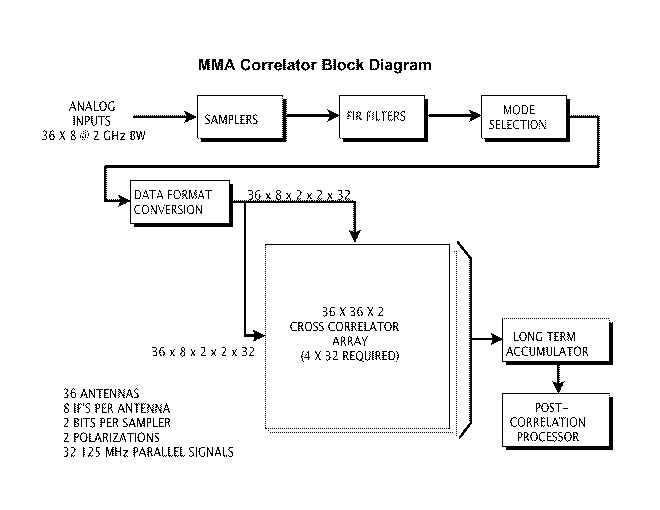
The correlator system envisioned for the MMA includes; the samplers (digitizers), digital filters, mode selection, a delay line and data format conversion stage, cross- and auto- correlators, long term accumulation, and initial digital computer processing. Depending on the mode of operation, the output of the correlator could be in either the lag or frequency domains.
A simplified block diagram for the MMA correlator is given in Figure 10.1. This diagram presents a fairly conventional lag correlator except for the presence of the data format conversion stage.
The analog outputs of the baseband system drive sampler inputs where 4-bit, 16-level sampling is performed at 4 GS/second. When less than 2 GHz bandwidth is desired, the samples are used as the input to the digital filter. The use of 4-bit quantization at the FIR filter input results in a negligibly small (~2%) loss of SNR; the output re-quantization to 2 bits provides suitable input to the correlator.
Logic in the mode selection block routes outputs from the digital filters into the data format conversion system. When fewer than 8 samplers per antenna are being used, this stage will assure high system efficiency by replicating active sampler outputs into unused memory areas and hence into otherwise unused correlators where additional lags can be generated. In this way, maximum performance will be obtained for the observational mode desired.
The digital filter stage will also do the sample decimation for observations in which sample rates less than 4 GS/second are needed. A 32-sample delay is required just before the digital filter in order to perform the finest resolution delay adjustment.
Adjusting the signals to the appropriate timing by means of a bulk delay is provided on the memory cards in very efficient high density RAMs. For a 30 KM delay range, 524,288 RAM bits per sampler output bit are required.
The data format conversion block seen in figure 10.1 will take the 32 parallel outputs of each sampler and, using RAMs, both adjust delays and re-sort the samples. In this block, the 32 parallel outputs of a high speed sampler would be converted from each carrying every 32nd sample to each carrying short (about 1 msec) bursts of contiguous samples. If the N-wide parallel (2-bit) output of a high speed sampler (each output carrying every Nth sample) were to drive the correlators using a conventional architecture, an N-by-N matrix of correlators would be required to insure every sample is correlated with every other sample. For N = 32, this would mean a matrix of 1024 small correlators to correlate the output of every baseband input of every baseline.
By using the format conversion scheme, the 32-wide parallel output from a high speed sampler will be transformed into 32 parallel signals each carrying 1 millisecond time segments of contiguous samples that need drive only an N-by-1 array of correlators. This simplification in the correlator circuit requirements is obtained at the cost of an inefficiency of about 0.2% which results because the end bits in adjacent 1 msec time segments of samples will not get correlated with each other.
(Note that the conversion from a conventional N-by-N architecture to an N-by-1 architecture does not improve the spectral resolution performance of the correlator. The performance is set by the number of hardware correlators in the system. The conversion does, however, greatly simplifying the system wiring in that all N-by-N signals from two antennas do not have to be wired to closely spaced electronics, thus simplifying the wiring matrix driving the cross correlators as well as reducing the number of I/O pins required by logic cards and integrated circuits.)
An additional benefit of the format conversion strategy is that it allows the system the same advantage as a recirculating correlator: when the bandwidth being processed is reduced by a factor of 2, the number of lags the system is capable of generating goes up by a factor of 2. This results in a factor of 4 increase in frequency resolution for a factor of 2 decrease in bandwidth.
Still another advantage of the format conversion (by far the most important in the MMA correlator) is that it allows a minimum cable interconnect complex between the station electronics and the correlators. It also eliminates any requirement to interconnect correlator arrays in low bandwidth modes. Since the number of data interfaces between these two stages in the MMA correlator surpasses that of any other astronomical correlator system by a factor of almost 100, this aspect of the system architecture is most important.
The cross correlator matrix of figure 10.1 is used to correlate the sampler outputs of every antenna with those of every other antenna. At the intersection of any antenna X and another antenna Y in this matrix, there will be a correlator chip. This correlator will compute lag products for the XY baseline while the antenna Y and antenna X intersection of the matrix computes the baseline lead products. Auto correlation products for each antenna are obtained from correlators on the matrix diagonal.
In order to minimize further the station electronics to cross-multiplier cable interconnect, a very compact cross correlator matrix is essential. The proposed design for the MMA correlator places an entire 40 X 40 cross correlator matrix (handling a 1/32, 125 MHz data rate, slice of the decimated sampler outputs) for two baseband inputs of opposite polarization on a single printed circuit card. This PC card in addition is configured such that no signal drives more than one load. For the number of signals required on a 40 antenna system, this property permits an absolute minimum cable matrix since every signal out of the station electronics goes one and only one place, driving only a single load.
One disadvantage of the proposed architecture is that once the number of antennas for the array has been set, future expansion of the correlator beyond this number is not practical.
The proposed custom lag correlator chip has a dual 4-by-4 array of correlators
(one for each of 2 polarizations). The chip can be programmed via a microprocessor
supplied program word for its position in the matrix and to select one
of three correlator configurations;
The estimated size of this custom correlator chip is in the 750,000
gate range.
For observations in which fewer than 8 baseband inputs are being used, more lags can be produced by dedicating more than one correlator array to process the outputs of active baseband inputs. In this case, cards in the data format conversion stage will be used to form a virtual connection, the effect of which is to link two or more correlator arrays in series. The delayed input to the correlator chips that are to compute the higher level lags will be displaced in time the appropriate number of bits by offset RAM addressing in the data format conversion cards.
The long term accumulation block seen in figure 10.1 integrates the correlator outputs for the desired duration. The correlator chips will produce a total of 52,428,800 lag results to be accumulated. The parallelism factor, 32, allows the reduction of this number to 1,638,400 which when double buffered and spread across 32 long term accumulator cards will require integration storage of 102,400 results per card.
The adoption of a digital FIR filter has a potential system-wide consequence: it makes more attractive the option of performing the digitization at the antenna and transmitting the data to the correlator over a digital rather an analog fiber optic link. This is due to the fact that, with analog filters, sampling at the antenna implies placing the analog filters at the antenna, with resulting stringent specifications on filter temperature stability which could be difficult to meet. The advantage of digitizing at the antenna is that the limited SNR and gain instability of an analog fiber optic link are eliminated. The disadvantages are possible shielding difficulties for the sampling clock and the (at present) high cost of digital transmission for 64 Gbit/sec data compared to the cost of two 8 GHz wide analog channels.
Bandwidths per baseband input range from a maximum of 2 GHz down in factor of 2 steps to 31.25 MHz. For 8 baseband inputs per antenna, this yields a maximum bandwidth per antenna of 16 GHz.
Sub-arrays will also be possible using the MMA correlator. The maximum number of sub-arrays for the MMA will not be determined by the correlator (that is, the MMA correlator will be able to support the maximum number of sub-arrays limited by other parts of the MMA).
There are assumed to be 8 samplers per antenna. The baseband inputs driving the samplers can consist of 4 dual polarization pairs or 8 independent inputs. For the case in which the baseband inputs come in polarization pairs, all 4 polarization cross-products may be computed. Each sampler is assumed to digitize at 4 GHz and hence to be driven by RF signals at most 2 GHz in bandwidth. The maximum bandwidth processed is thus 16 GHz split into 2 GHz pieces. Note that the analog baseband constraints of the planned MMA baseband processing system will impose limits as well.
The smallest division of lags in the projected correlator chip is 64 lags. Because of the architecture proposed, this will produce 64 lead and 64 lag channels and hence 64 spectral points per product. This smallest correlator division means that in the full-up configuration, all baseband inputs active at maximum bandwidth and all 4 polarization products being computed, 64 spectral points will be produced for every baseline, every spectrum. This gives a frequency resolution per spectral channel of 31.25 MHz.
Given the full-up performance as defined above, the number of lags that
the proposed correlator can produce for a given experiment results from
the following considerations:
2. If fewer than 8 baseband inputs are required, lags go up as 1 over the fraction of baseband inputs used (1/2 the baseband inputs, 2 times the lags).
3. If a lower bandwidth than 2 GHz per baseband input is required, lags go as 1 over the fraction of maximum bandwidth (1/4 the maximum bandwidth, 4 times the lags) until a factor of 32 is reached. After that, the number of lags stays constant. The particular configuration can be selected on an baseband by baseband basis.
Note that item 3 implies the characteristic described above that
for each reduction by a factor of 2 in bandwidth, an increase of a factor
of 4 in resolution is obtained (up to the factor of 32 limit after which
the resolution improves by only 2 for each factor of 2 reduction in bandwidth).
Table 10.3 below illustrates some of the possible modes. The first four columns relate to the correlator proper. The columns relating to velocity range and resolution assume 90% of the analog bandwidth will be usable. (See MMA memo 194 for additional illustration of the MMA correlator performance.)
|
|
Sampler |
Products? |
Product |
Range
Resolution
|
|
|
|
|
|
|
|
|
|
|
|
|
|
|
|
|
|
|
|
|
|
|
|
|
|
|
|
|
|
|
|
|
|
|
|
|
|
|
|
|
|
|
|
|
|
|
|
|
|
|
|
|
|
|
|
|
|
|
|
|
|
|
|
|
|
|
|
|
|
|
|
|
|
|
|
|
|
|
|
|
|
|
|
|
|
|
|
|
|
|
|
|
|
|
|
|
|
|
|
|
|
|
|
|
|
|
|
|
|
|
|
|
|
|
|
|
|
|
|
|
|
|
|
|
|
|
|
|
|
|
|
|
|
|
|
|
It is estimated that the station-dependent part of the system (sampler, filter, mode, and memory) will require 1/2 a rack per antenna, or 20 racks for 40 antennas. The remainder of the system, proportional to the number of antennas squared (correlator, control, and accumulator) will occupy 8 racks for 40 antennas. The grand total of racks is therefore about 28.
By using low voltage chip technology it is hoped that the custom correlator chip described in this document can be built with about a 2 or 3 watt power requirement. The chip represents about a factor 2 increase in the level of integration when compared to the GBT correlator chip (twice the number of transistors). By using a more modern process, with finer component features and low voltage technology, a smaller chip with lower power requirements should be possible. The smaller silicon size should also mean a higher yield in the manufacturing process.