MMA Project Book, Chapter 8
SYSTEM DESIGN OVERVIEW
Richard Thompson
Last revised 1998-Nov-14.
1998-11-12, addition of sections 8.1-8.3, summaries of specifications, goals and milestones.
8.1 TOP LEVEL SPECIFICATIONS
1. Provision for up to 10 frequency bands (i.e. to handle outputs of up to 10 receivers).
2. Maximum IF bandwidth 16 GHz per antenna, to be subdivided into eight bands, each 2 GHz wide.
Choice of assignment of the eight bands between two polarizations, and for SIS receivers between upper and lower sidebands, to be provided.
3. The 2 GHz bandwidth to be adjustable downwards in factor-of-two steps to 31.25 MHz, as desired, for the correlator input.
4. The 16 IF bands from each antenna to be converted to four-level digital form as input to the correlator system.
5. Local oscillator signals to allow for full tunability of IF bands across receiver bands.
6. LO system to allow tunability in increments small compared with the narrowest IF filter bandwidth (i.e. approximately 5 MHz, but exact figure to be chosen for convenience in LO design).
7. Provision of phase switching on first LO by 90 and 180 steps.
8. Provision of frequency offsets for fringe rotation on the first LO and a later one.
8.2 GOALS AND OPTIONS
1. Overall goal of systems development is to test concepts for signal paths from receiver outputs to correlator input, including the required LO system, associated monitor and control, etc.
2. Option: location of samplers for A/D conversion of signals. Base plan is to bring signals from antennas in analog form and digitize at Electronics building. Alternate plan is to digitize at antennas and to transmit to Electronics building in digital form.
3. Verify concept of switching system for selection of signals from different receivers ( Fig.2). In particular, that IF response can be maintained sufficiently flat (˜ 1dB) over 2 GHz band.
4. Option: Baseband Converter design. Preferred design is the one using digital filtering (Fig. 5). Digital filter needs hardware verification. Alternate design uses analog filters (Fig. 4).
5. Option: First LO implementation. Preferred design is photonic system. Alternate is "conventional" design (Fig. 7) with transmission of reference frequencies to antenna for synthesis of LO.
6. Test stability of total power measurement used for observation in single-antenna mode. Will require tests on antenna because requirement is related to antenna performance (beam switching).
7. Verify number of optical fibers required per antenna, allowing for spares and future expansion.
8.3 MAJOR MILESTONES
1. Decision on digital or analog filters in Baseband Converter. This decision milestone is set for 1998-12-31, WBS 8.5.3.3.
2. Decision on photonic or conventional first LO. This decision milestone is set for 2000-06-30, WBS 5.6.
3. Completion and laboratory test of complete IF channel from receiver to correlator.
The delivery date for this is 2001-01-31, WBS 6.8.
8.4 INTRODUCTION
The part of the system considered here includes the signal paths from the outputs of the front ends to the digital samplers, and the local oscillator (LO) system, but it does not include details of the front ends, the digital delays or the correlator. The purpose of this chapter is to provide a general description of the signal paths from the receiving front ends to the correlator, and the distribution of local oscillator and monitor-and-control signals to all parts of the system as required.
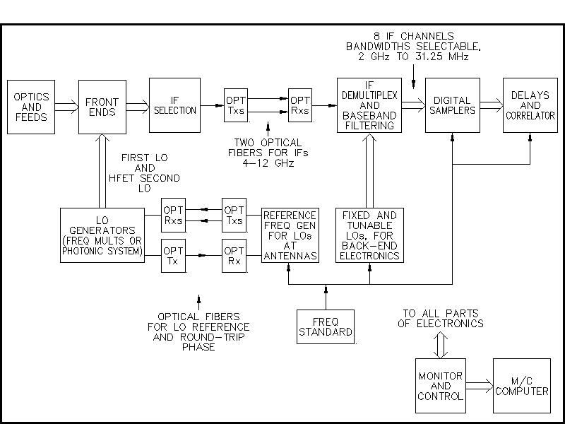
A simplified block diagram of the overall system is shown in Fig. 1. Components at the left-hand side of the optical fibers in the IF and LO paths are located at the antennas and those at the right-hand side are in the Electronics Building which is located close to the array. At each antenna there are ten receiver front ends which receive signals from Cassegrain feeds. The input stages use HFET (heterostructure field-effect transistor) amplifiers at frequencies from 30 to approximately 115 GHz and SIS (superconductor-insulator-superconductor) mixers for higher frequency bands up to 950 GHz. Two orthogonal polarizations are observed simultaneously, so there are two IF outputs from each HFET front end. For each SIS front end there are four outputs since the mixers will also provide separate outputs for the upper and lower sidebands. The IF signals transmitted from each antenna to the Electronics Building where the correlator is located will consist of two bands each 8 GHz wide, one for each polarization. The 8-GHz bandwidth is the widest that is deemed practicable considering limiting factors which include the need to keep the noise temperature of the SIS-mixer input stages as low as possible, and the processing capacity of the correlator (MMA Memo. 166, Memo. 194). The IF band is tentatively chosen as 4-12 GHz to keep frequencies low while also keeping the relative bandwidth less than two octaves to allow satisfactory performance for components such as the IF hybrids which are used in the sideband separating mixers.
During the IF processing the signals are digitized and the insertion of compensating time delays and the cross-correlation of the signals from pairs of antennas is performed digitally. An important question is the location of the analog-to-digital (A/D) conversion in the data streams from the antennas to the correlator, in particular, whether the signals are transmitted from the antennas in analog or digital form. A/D conversion at the antennas considerably increases the complexity of the electronics at the antennas, which is undesirable because maintenance is most easily performed for equipment located in the Electronics Building. The stability of the frequency response of the overall analog system is an important factor in the performance of the array, and with analog transmission this includes the frequency response of the fiber optic system. However, it is very difficult to predict the degradation in performance, if any, that would result from analog transmission. The two 8-GHz-wide bands from each antenna can be transmitted as analog signals on two fibers. For digital transmission of the IF signals, with four-level digitization (two bits per sample), the total data rate from each antenna would be 64 Gb/s. Transmission of digital data would thus require more bandwidth than is needed for the signals in analog form. The present decision is to use analog transmission for the prototype test array, as described here. A more extensive discussion of the analog/digital transmission question can be found in MMA Memo. 142.
At the Electronics Building the two 8-GHz-wide IF bands from each antenna are split into four baseband channels, each 2 GHz wide. These are passed through filters that allow the bandwidth to be varied in factors of two, digitized, delayed and cross-correlated. A frequency standard and various synthesizers provide the reference frequencies for various local oscillators and for timing of the digital units. For the LOs at the antennas, standard frequencies are generated at the Electronics Building and transmitted to the antennas on optical fibers. A separate fiber is provided for measurement of the round-trip phase. Appropriate phase switching and fringe-frequency phase rotation are inserted through to LO system. A monitor and control system interacts with all parts of the electronics.
8.5 SIGNAL PATHS AT THE ANTENNAS
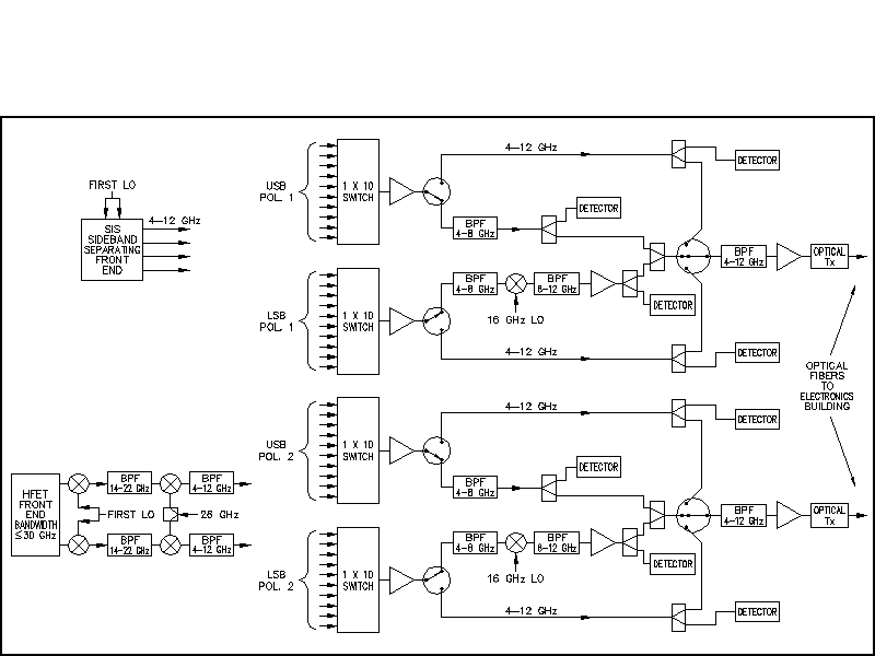
Figure 2 shows the system at the antennas. Note that the diagrams indicate the signal flow by showing mainly filters, mixers and switches, and other components will be found in the detailed design descriptions. Each of the four IF outputs from each SIS-mixer front end goes to one of four 1x10 switches. An IF band spanning 4 to 12 GHz (that is, a bandwidth of 8 GHz) is used for each of the two opposite polarizations received. An SIS mixer with a 4 GHz IF bandwidth and good noise temperature has been demonstrated (Padin et al. 1996) using an IF stage integrated with the mixer. It is believed that 8 GHz bandwidth is an achievable goal within the construction period of the MMA. However, in the shorter term the noise temperature of SIS front ends matched to a 4 GHz bandwidth may be better than those matched to the full 8 GHz bandwidth. Thus, instead of two 8-GHz-wide bands it may be preferable to use four 4-GHz-wide bands from each SIS front end (that is, both polarizations for upper and lower sidebands) in order to maximize the sensitivity. By means of the four 1x2 and two 1x3 switches shown in Fig. 2, the input to each optical transmitter can be selected to come from either one 4-12 GHz front end output or two 4-8 GHz front end outputs, one of the latter being converted to 8-12 GHz for transmission on the fiber. It is hoped to simplify this switching arrangement during the development phase since, in practice, the deviations of the IF passband from flatness can be expected to increase with the number of interconnections.
Figure 2: System at each antenna
The maximum bandwidth of any of the HFET front end is approximately 26 GHz. The first IF band for the HFET front ends is 14 to 22 GHz, so there is a frequency gap of 28 GHz between the upper and lower sideband responses at the mixer that converts to the first IF. Thus for most HFET front ends it should be possible to avoid image responses if a filter is included to confine the amplifier response to the nominal band. However, two frequency conversions are required to get to from the HFET input frequency to the 8-12 GHz IF band. Note that the IF band 14-22 GHz is chosen to be about as low in frequency as is possible to use while avoiding direct feed-through to the 4-12 GHz band. For reasons of cost it is preferable to keep intermediate frequencies as low as possible, but the IF bandwidths required place lower limits on the frequencies because of the need to avoid image responses, etc.
The arrangement of switches shown in Fig. 2 is one of several possibilities and the final system design will have to take into account the availability and cost of different types of switches, and the effect of their loss and reflections on the flatness of the IF response. Some modes of operation of the array may require continuous switching between two front ends at intervals as short as 10 s, so mechanical switches with limited switching-cycle lifetimes would not be suitable. The switches should be mounted within the front-end Dewar to minimize the number of coaxial lines that have to pass through the Dewar wall. The switches should be cooled to 15K to minimize the heat leakage into the cryogenically cooled components. It is not clear that coolable GaAs switches with sufficient bandwidth are available. Thus as an alternative which is being considered is the use of power combiners to replace the switches. The power combiners would be cryogenically coolable and front ends not in use would be switched off by removing power from their output stages. Since there would be a 10 dB loss in signals passing through a 10-way combiner, a corresponding increase in IF gain would be necessary.
8.6 SIGNAL PROCESSING AT THE ELECTRONICS BUILDING
Each of the 4-12 GHz IF bands is demultiplexed into four 2 GHz-wide bands when received at the Electronics Building, and these are all converted to a frequency of 2-4 GHz, as shown in Fig. 3. Demultipexing to bandwidths of 2 GHz allows the use of a clock frequency of 4 GHz for the samplers, which is within the state of the art but requires some development. Also the problem of keeping the overall bandpass characteristic uniform within approximately ˜1 dB is simplified since the narrower 2-GHz bandwidths can be considered individually. The 2-4 GHz IF bands then go to individual Baseband Converter units, of which four are required per polarization for each antenna. A switching network allows the four IF bands for a given polarization to be connected to four Baseband Converter inputs in any manner desired. For example, all four Baseband Converters may be connected to one 2 GHz-wide IF band if it is desired to study four narrow lines that all lie within the same 2 GHz-wide band.
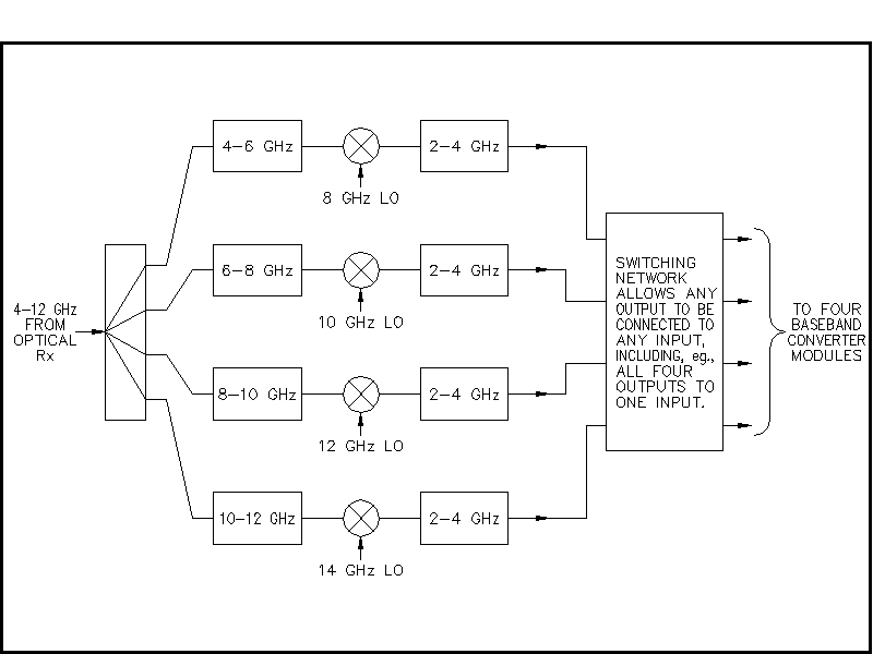
Figure 3: Demultiplexing the 2-GHz bands
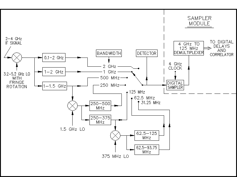
Figure 4: Baseband Converter
In the Baseband Converter unit in Fig. 4, the input signal at 2-4 GHz is converted to the baseband range and filters are provided for selection of bandwidths from 2 GHz down to 31.25 MHz in steps of a factor of two. Just ahead of the Baseband Converters the signals pass through the 2-4 GHz filters shown in Fig. 3. When converting the full 2 GHz bandwidth to baseband using a 4 GHz LO, frequencies above 4 GHz can get converted to frequencies at the low end of the baseband range. To minimize this effect the 2-4 GHz filters in the Baseband Converters should have a sharp response at the 4 GHz edge. The low frequency cutoff of the 0.1-2 GHz filter is also intended to help reduce such unwanted frequencies. The 1-2 and 1-1.5 GHz filters are far enough away from the low end of the 0.1-2 GHz baseband to be free from such unwanted effects. Similarly, the two frequency bands following each of the 1.5 GHz and 375 MHz LOs are well above zero frequency and will not include unwanted components from spectrum fold-over at an LO frequency. The reason for the variable bandwidth is that in the correlator the frequency resolution is increased as the total bandwidth to be processed is reduced. The 3.2-5.2 GHz LO at the first frequency conversion is tunable to allow the response of the baseband converter to be set at any part of the 2-GHz-wide IF input band. Thus for observations of spectral-line features the baseband responses can be adjusted in frequency and bandwidth to suit the characteristics of the line involved. In designing the Baseband Converter, it was decided to use a system involving a number of frequency conversions with filters chosen to reject the unwanted sideband responses, rather than using a sideband-separating mixer because the latter, although simpler, does not provide sufficient rejection of unwanted sidebands. Unwanted responses from other lines should be reduced by at least 40 dB. Table 1 lists the bandwidth of each filter, the frequency range of the passband as seen at the output of the first mixer (the one with the 3.2-5.2 GHz LO), and the tuning range of the LO which just covers the 2-4 GHz input band in each case. Image responses fall above 4 GHz in all cases.
| Bandwidth | Filter response as seen
at output of first mixer |
LO tuning range |
| 1.9 GHz | 0.1-2.0 GHz | 4.0 GHz |
| 1.0 GHz | 1.0-2.0 GHz | 4.0-5.0 GHz |
| 500 MHz | 1.0-1.5 GHz | 3.5-5.0 GHz |
| 250 MHz | 1.0-1.25 GHz | 3.25-5.0 GHz |
| 125 MHz | 1.125-1.25 GHz | 3.25-5.125 GHz |
| 62.5 MHz | 1.1875-1.250 GHz | 3.25-5.1875 GHz |
| 31.25 MHz | 1.1875- 1.21875 GHz | 3.21875-5.1875 GHz |
The fractional bandwidths of the filters, other than the two widest ones, are in the range 0.4 to 0.67. Note that if the chosen output band comes from one of the three widest filters, the input of the 1.5 GHz LO signal to the module should, if necessary, be turned off to prevent pickup of this LO frequency in the earlier filters. Similarly, unless one of the two narrowest bandwidths is being used the 375 MHz signal should be switched off. The filtered outputs are sampled at a 4 GHz clock rate and digitized. The 4 Gb/s digital data streams from the samplers are each demultiplexed into 32 bit streams at 125 Mb/s and then go to the delay and correlator system. Redundant samples for the bandwidths of 1 GHz and less are removed as necessary at an appropriate stage. Eight Baseband Converter units are required for each antenna.
An alternative to the Baseband Converter module in Fig. 4 is the digital filter scheme shown in Fig. 5. Here the IF signal is sampled at its full bandwidth, and then the filtering is implemented digitally. Each 4 Gb/s output stream of the sampler is multiplexed into 32 bit streams at 125 Mb/s, which is the clock rate for the correlator and would also be used for the digital filters. Filter design is based on the FIR (finite impulse response) type, and discussed in more detail in MMA Memo. 204. The incoming sample stream is fed through two-bit shift register, the length of which is tentatively chosen as 128 samples. Each stage of the shift register is assigned a number, referred to as a tap weight, by which the sample in the particular stage is multiplied. At each clock cycle the samples are multiplied by the tap weights corresponding to their positions in the shift register, and the products are summed and form one sample of the filtered output signal. At the next clock cycle each sample moves to the next stage of the shift register and the multiplication by tap weights and addition are repeated. It will be seen that in the time domain the series of summed products represent a sampled convolution of the input IF signal with a function represented by the series of tap weights. Thus, in the frequency domain the output stream represents the IF input spectrum multiplied by the Fourier transform of the tap weight function. The tap weights can be stored in a random-access memory (RAM) and different sets of values can be entered to provide different filter characteristics as required.
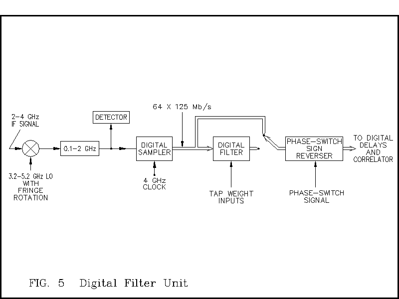
Figure 5: Digital Filter option
The fact that the sampled data are represented by only four levels results in an important simplification, since the multiplication of one data sample by a particular tap weight can result in only one of four different values, and these can be stored as a look-up table in a RAM. The multiplication is then replaced by selection of the appropriate value. Note that as the filter bandwidth is halved the output sample rate is also halved, which, in effect, allows the data to be recirculated through the shift registers, doubling the effective number of tap weights.
The advantages of digital filtering are that the accuracy of the phase and frequency responses depends mainly on the timing accuracy of the digital circuitry, which allows greatly reduced dependence on temperature stability and better matching of responses for different IF signals. The ability to change the tap weights allows one set of digital filter circuits to provide many different responses. The use of digital transmission of the signals from the antennas would be simplified, since digital filtering allows the filters to remain at the correlator, and only the samplers need be moved to the antennas. Thus stability and flexibility are enhanced, and there should also be some cost saving. A disadvantage of digital filtering is that the output samples resulting from the tap-weight multiplication and addition are represented by multi-bit numbers. The number of bits then has to be reduced to whatever the correlator will accept, which is only two bits as presently conceived. The truncation of the data results in the quantization loss occurring twice, once at the sampler and once in the truncation. This additional loss need not occur when the full IF bandwidth is used since the digital filter can then be bypassed. A proposed digital filter implementation, as described in MMA Memo. 204, would require development of a custom, large-scale, integrated circuit but this would not so large and complicated as that for the correlator.
The digital filter will be pursued by computer simulation, followed by chip design. the goal would be to have a tested design for the array construction phase, but for the test antenna the more conventional design of Fig. 4 will be used.
8.7 TOTAL POWER OBSERVATIONS AND SIGNAL LEVEL CONTROL
In the IF system at the antennas, (Fig. 2), detectors are shown which measure the IF signal level in the 4-GHz-wide and 8-GHz-wide bands at the inputs to the optical transmitters. In the Baseband Converter (Fig. 4) and digital filter module (Fig. 5) a detector is shown which measures the level of the signal going to the digital sampler. These detectors perform two functions. First, they can be used for total power measurements. Those at the antenna would be used for wide-band continuum measurements. For total power measurements in spectral line mode the autocorrelation outputs of the correlators are required. Note that if SIS mixers with the full 8 GHz bandwidth prove feasible, then at the antennas it is possible to make total power measurements on all four 4-12 GHz outputs of an SIS front end simultaneously, thus making use of twice the bandwidth that is available in interferometer mode.
The second use of the detectors is to check the IF signal level at two points where it is particularly critical. One of these is the inputs to the optical transmitters in which nonlinearity can occur if the level is too high, and loss of signal-to-noise ratio can occur if the level is too low. The other point is the input of the digitizing sampler where it is necessary to know the rms input noise level in terms of the A/D reference levels. A variable attenuator or a variable-gain amplifier (not shown in the figures) will be included in the signal path ahead of each detector. These gain controls and the detector outputs will be accessible through the monitor and control (M/C) system. Thus various control schemes including adjustment in discrete steps, full ALC (automatic level control), sample-and-hold, etc. can be implemented through a control computer. If on-the-fly mapping or subreflector nutation are used in observing, then it may be necessary to measure and control the gain for a particular reference direction of the antenna beam.
8.8 PHASE SWITCHING AND FRINGE ROTATION
SIS mixers incorporating sideband separation are being developed for the MMA, but it is expected that it will be possible to achieve only 10-15 dB of isolation between the sidebands. This is sufficient to eliminate the noise from the unwanted sideband to a satisfactory degree. However, spectral dynamic range at least as high as 40 dB is desirable, so it is also necessary to include sideband separation. This is often performed by means of by 90 phase switching, but there are advantages to using a fringe-frequency offset scheme suggested by B. G. Clark. In either of these schemes phase adjustment must be applied to the first LO. In correlator arrays it is also generally useful to incorporate 180 phase switching to reduce effects such as unsymmetrical offsets in the sampler reference levels and spurious responses from unwanted signals that infiltrate the IF stages.
To explain the frequency offset scheme for sideband separation, consider first just two elements of the array. The fringe frequency can be brought to zero, that is the fringes can be stopped, by adding a frequency offset to the first local oscillator at one antenna, and a smaller frequency offset to a later LO. In the MMA we plan to use the 3.2-5.2 GHz LO shown in Figs. 4 and 5 for the second of these offsets. The offsets compensate for the variation of the delay between the time that a wave front from a source under investigation reaches one antenna and then the other. Suppose that, in addition to the fringe stopping phase shifts we also add a frequency f1 to the first LO of one antenna. Then the fringe frequency at the correlator output becomes equal to f1 for both sidebands. Now if we subtract f1 from the frequency of the LO with the second fringe-stopping offset, then the result will be that the fringe frequency at the correlator becomes zero for one sideband and 2f1 for the other sideband. If 1/( 2f1 )is large compared with the averaging time at the correlator output, the fringes will average to a very low residual leaving the full response for the sideband for which the fringes were stopped. The averaging can be made most effective by choosing f1 such that there are an integral number of fringe cycles in an averaging interval. One can select either sideband to be the one that is retained by either adding or subtracting f1, as appropriate, at the later LO. This is illustrated in Figure 6.
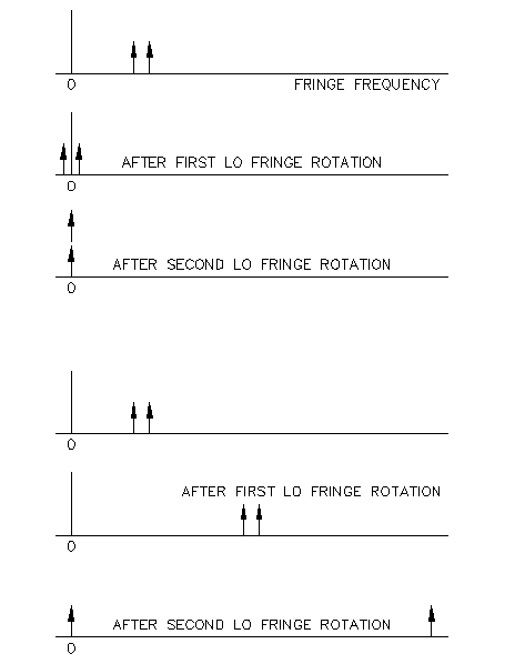
Figure 6: Fringe rotation and the sideband separation scheme
The upper half of the diagram shows how the fringes of both sidebands can be stopped in a double sideband system. The natural fringe frequency of the two sidebands is shown by the two arrows at the top. An offset on the first LO is then used to move the fringe frequencies so that they are centered on zero: at this point the fringes can be envisaged as the projection on the real axis of two contra-rotating vectors in the complex plane. An offset on a later LO brings the two fringe frequencies to zero. The lower half of the diagram shows how the fringe frequency can be brought to zero for one sideband and, for the other sideband, brought to a high frequency that is removed in the time averaging at the correlator output.
In applying the above scheme to an array of Na antennas, the offset frequency must be different for each antenna. This is easily achieved by making the offset equal to N1 for antenna N, where N takes values from 0 to (Na-1). Although this sideband separation process results in the loss of one sideband, it fits the MMA requirement well because the SIS mixers that will be used will be designed to separate the sidebands, but will provide only 10-15 dB of rejection. The fringe offset scheme described here is required to increase the suppression of the unwanted sideband which has already suffered limited rejection at the mixer. Note that the reason for using the sideband separating mixers is that they suppress the noise from the unwanted sideband, which the LO offset scheme does not do. Thus the sideband separation in the mixer increases the sensitivity by a factor that depends upon the antenna temperature, and may be as high a two. The variable frequency LOs are required for fringe stopping, whether or not the above scheme is used for suppression of an unwanted sideband. Thus no additional hardware, but some software, is required to implement this method.
Phase switching by 180 degrees is required to eliminate responses to possible spurious signals and to correct for nonsymmetrical errors in the quantization thresholds of the samplers. It is necessary that the switching waveforms between any two antennas be orthogonal. Switching sequences based on Walsh functions allow this condition to be achieved with a smaller range of transitions per second than would be possible with squarewaves. The phase switching should be inserted at the first LO and removed after digitization by sign reversal in the 125 Mb/s data streams. The timing of the Walsh function transitions should be such that for the signals from all antennas the transitions are in phase at the input to the correlator. After the IF signals are digitized, a variable digital delay is used to compensate for the variation of the arrival time of a wave front at the different antennas, and this should be taken into account in the timing of the transitions when the Walsh functions are inserted at the antennas. Maintaining the correct timing can require some extra hardware and software when using very short averaging times and/or long baselines. If the phase switching is found to be necessary only to correct for non-symmetrical quantization thresholds, then it should be possible to replace it by automatic control of the threshold levels. For four-level sampling, the dc level of the sampled waveform would be adjusted to equalize the total numbers of positive and negative samples, and the quantization levels would be adjusted to equalize the numbers of positive and negative high-level counts. Counters for the four sampling levels would provide inputs to digital-to-analog converters to provide the dc levels. Such a scheme may be examined as part of the two-element prototype testing.
The LO fine tuning required for introducing fringe frequency offsets may also be used for fine adjustment for Doppler shifts, to allow data taken at different times to be combined. Thus the range of the offsets provided for fringe rotation should be as wide as the narrowest tuning interval provided by any other LO, to provide complete frequency flexibility. Alternatively, Doppler shifts can be removed by interpolation of the spectra at the correlator output.
8.9 THE LOCAL OSCILLATOR SYSTEM
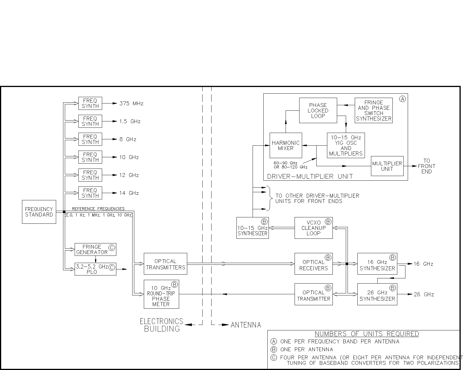
A scheme for the local oscillator system based on the use of conventional frequency multipliers is shown in Fig. 7. A frequency standard provides inputs for various synthesizers and other units. The double line between blocks indicates multiple signal paths carrying several frequencies, such as 1 Hz, 1 MHz, 1 GHz, and 10 GHz. The final values for these reference frequencies will be chosen to take account of the design details of the synthesizer units for which they are required. The synthesizers at the top left of the figure provide the two fixed frequencies (375 MHz and 1.5 GHz) required by the Baseband Converters (Fig. 4). These two frequencies would not be required with the digital filtering scheme in Fig. 5. The four synthesizers immediately below them provide the four LO signals required by the Demultiplexer units in Fig. 3. In the lower left part of Fig. 5 there are units designated 3.2-5.2 GHz synthesizers. These produce the 3.2-5.2 GHz LO signals with frequency offsets for fringe rotation and sideband separation that are used in the Baseband Converters in Fig. 4. Each of the 3.2-5.2 GHz Synthesizer units receives a signal from a fringe generator which uses a number-controlled oscillator or similar device to produce a signal at some convenient low frequency, such as 1 MHz, with the required offset for fringe rotation and sideband separation. This frequency is then combined with the synthesizer output.
Click on image to zoom
Figure 7: Local oscillator scheme using conventional frequency multipliers
The other part of the local oscillator system in Fig. 5 is concerned with the LOs required at the antenna. In the lower right area, fixed-frequency synthesizers at the antenna produce 26 GHz for the second LO for the HFET front ends and 16 GHz to convert 4-8 GHz IF bands to 8-12 GHz. The 10 GHz reference frequency is returned to the Electronics Building on a separate fiber to provide a round-trip phase measurement. The phase of the returned 10 GHz signal is measured with respect to the outgoing signal to monitor changes in the total path length of the fiber between the Electronics Building and an antenna. Thermally induced path-length variations usually result more from the fiber runs up the antennas than from the longer buried sections. It can be assumed with some degree of accuracy that all fibers going to an antenna will be in a similar environment and suffer similar thermal expansion.
In Fig. 7 a system of multipliers for the first LO system is in the upper right area. The unit labeled "10-15 GHz YIG oscillator and multipliers" (in the Driver-Multiplier unit) produces the 6th or 8th harmonics of a 10-15 GHz YIG oscillator (60-90 or 80-120 GHz), and this is amplified to a level of no less than 50 mW. This frequency is locked to the corresponding harmonic of a synthesizer that uses a fixed reference frequency which has been filtered by means of a phase-locked loop containing a crystal oscillator. The phase-locked loop for the YIG oscillator uses a phase reference that contains the required frequency offsets and phase changes for the fringe rotation, sideband separation, and phase switching. The 60-90 GHz and 80-120 GHz signals are sufficient to drive multipliers that can supply the first LO for any of the front ends above 60 GHz. For lower frequency front ends, an LO signal can be brought out from an earlier stage of the multiplier chains. Note that the frequencies in the multiplier chains are too high for switches other than waveguide type and these are deemed undesirable because of expense and also because experience shows that they do not always reset with sufficient mechanical precision, resulting in reflections and phase errors. Thus a separate Driver-Multiplier unit is required for each of the ten front end bands at each antenna. However, the output of the fringe and phase switch synthesizer, shown in the Driver-Multiplier unit, can be switched and shared between the Driver-Multiplier units at an antenna. It is expected that the multiplier scheme will be used for the two-antenna test array to be constructed during the development phase of the project.
A photonic LO system is being investigated as an alternative for the high frequency first LOs in the MMA ( MMA Memo. 200 ). Two optical signals that differ in frequency by the first LO frequency are transmitted to the antenna on a single fiber. These are then combined in a photodiode resulting in enough power to drive an SIS mixer. The lasers that generate the optical signals for each antenna are located at the Electronics Building. If the photonic scheme proves practicable, it will greatly simplify the electronics since the requirement for frequency multipliers producing power levels sufficient to drive the mixers will be eliminated. Also, switching the LO signal to different front ends can be done using an optical fiber switch, and will eliminate the requirement of a separate Driver-Multiplier unit for each frequency band at an antenna. It has been suggested that a similar scheme should be used to produce correlated phase-calibration signals at the antennas. If this proves successful the round-trip phase measurement should be moved from the LO system to the calibration system.
8.10 DISPERSION IN THE OPTICAL FIBER
The optical transmitters for the IF signals will use external modulators to avoid causing frequency modulation of the laser. The optical frequency of the laser at 1300 nm wavelength is 2.3 x 10¹⁴ Hz, and a 2 GHz-wide IF signal spans 0.011 nm in wavelength. Assume that the laser wavelength is within 20 nm of the zero-dispersion point of the fiber, so that the dispersion is no more than 1.5 ps/nm.km. For standard fiber the zero dispersion point is near 1300 nm. Then for 25 km of fiber, which is approximately the longest fiber run from an antenna to the Electronics Building, the time difference for frequencies at the edges of a 2 GHz-wide band is no more than 0.41ps, which corresponds to 0.3of phase at 2 GHz. This is the effect of the dispersion on the intrinsic bandwidth of the IF signal. One can conclude that any resulting loss in coherence between an IF band that has traversed 25 km of fiber and one that has not can be neglected. Now consider the effect of variation of the laser wavelength, which is a function of temperature. If the laser wavelength changes by 0.013 nm, that is by 1 parts in 105, and again the dispersion is about 1.5 ps/nm.km, then the time for traversal of 25 km of fiber changes by 0.49 ps. This can be compared with the minimum increment in the compensating delay in the system which we will take to be 1/32 of the reciprocal bandwidth at the sampler (the same as in the VLA), which is 15.6 ps. Thus again the error is small enough to be tolerable. Note that if we used a laser wavelength of 1550 nm, the dispersion in standard fiber would be approximately 15 ps/nm.km, that is, a factor of 10 greater. For IF transmission the dispersion would still be just about tolerable, but one would not want it to be much greater.
The effects of variation in the effective length of the fiber on the LO signals must also be considered. A change in delay of 0.49 ps, resulting from a drift in the laser wavelength, corresponds to a phase error of 0.4 turns (144) at 800 GHz. The effect of a slow variation of this magnitude over several hours would be removed by frequent switching to a calibrator source, which is required in any case to correct for atmospheric effects. If one used standard fiber and a laser wavelength of 1550 nm the same laser wavelength drift would result in 4 turns of phase change at 800 GHz.
The loss in standard single mode fiber is about 0.35 dB/km at 1300 nm and about 0.2 dB/km at 1550 nm. Also, optical amplifiers are more readily available at 1550 nm. However, the dispersion is about 15 ps/nm.km at 1550 nm, whereas it is near zero for a laser wavelength of 1300 nm. Dispersion-shifted fiber in which the zero-dispersion point is shifted to 1550 nm is also available. An enquiry to Optical Cable Corporation reveals that the price of dispersion-shifted fiber is about 50% more than standard fiber, but that they could supply multi-fiber cable with, say, one fourth of the fibers of dispersion-shifted type, for a correspondingly smaller cost increase. Thus the advantage of using dispersion-shifted fiber for the local oscillator reference signals should be examined.
Variations in the effective length of a fiber can be monitored by a round-trip phase measuring system. Round-trip phase systems have been satisfactorily demonstrated in fiber optic transmission, using either the same fiber as the outgoing signal, or a separate fiber (Webber and Thacker 1990), for the returned signal. Here again the effects of the wavelength stability of the lasers and the dispersion in the fiber on the overall accuracy should be considered. Tests to determine the best way to design and implement a round-trip phase measurement to improve the instrumental phase effects for the MMA should be part of the development phase of the project.
8.11 ACKNOWLEDGMENTS
Members of the MMA Systems group who have contributed to the discussions on which this system plan is based include D. S. Bagri, J. E. Carlstrom, B. G. Clark, L. R. D'Addario, D. Emerson, R. P. Escoffier, P. J. Napier, S. Padin, J. D. Romney, R. A. Sramek, D. D. Thornton, J. C. Webber, and W. J. Welch.
8.12 REFERENCES
S. Padin, D. P. Woody, J. A. Stern, H. G. Leduc, R. Blundell, C.-Y. E. Tong, and M. W. Pospieszalski, An Integrated SIS Mixer and HEMT Amplifier, IEEE Trans. Microwave Theory Tech., 44, pp. 987-990, 1996.
J. C. Webber and D. L. Thacker, Phase Distribution on Fiber Optic Cable, Report prepared by Interferometrics, Inc. for Naval Research Laboratory, May 3, 1990.